|
|||||||||||||||||||
Parts Solutions
Sac-Tec supports all custom packaged microcircuits and obsolete and sunset technologies.
| Custom Packaged Microcircuits | |
 SAC-TEC supports all forms of semiconductor and microcircuit technologies from simple 2-pin diodes to complex 256-pin high-density semiconductors. SAC-TEC is one of only a few build-to-print manufacturers nationwide capable of producing Hi-Rel custom components specialized for the Aerospace market place. The Hi-Rel nature of military and space applications requires strict processing standards. Source Control Drawings (SCD) further refine these standards to specific product processing specifications demanded by unique system designs. SAC-TEC can offer both standard or customized process flows tailored to the Hi-Rel applications of our customers. What is a Custom Package? A custom package is the encapsulation of a desired semiconductor or microcircuit in high reliability housings. These special housings are designed to meet or enhance a semiconductor's performance. Many new power devices coming to market require special cooled surfaces or connections to maximize component thermal characteristics. SAC-TEC, provides unique metal or ceramic housings to meet each customer's mechanical, thermal, or power handling needs. Today, many state-of-the-art microcircuits are released in plastic cases, which serve only commercial or industrial uses. These same microcircuits can be obtained by SAC-TEC in die form and assembled into Hi-Rel, hermetic, metal or ceramic housings for operation under adverse conditions. Why Use Custom Packages? (The missing design link) Every electronic application has fit, form, and function problems associated with circuitry layout, required performance or standardization in production capabilities. Custom-packaged microcircuits either fill voids in today's manufacturing system designs, or provide a competitive edge to companies competing in the military marketplace. Most semiconductors and microcircuits used in the Aerospace sector require better thermal characteristics, smaller footprints, improved electrical characteristics, or guaranteed radiation hardness. Only by customizing these components can design engineers maximize their system's performance. SAC-TEC provides variations and trade-offs in packaging technology, which can meet customers' optimal design goals. When Time is of the Essence Because a $ 100 million satellite must stay grounded until every component is delivered, controlling the project time clock is often critical in custom packaging. Over and over, SAC-TEC has rescued projects from late delivery by exercising emergency product builds. A component which may take up to 50 weeks to finally ship from major semiconductor OEMs can normally be delivered from SAC-TEC in 20 weeks or less. SAC-TEC has, under severe conditions, delivered a Class S product in 7 weeks.
|
|
| Is Custom
Packaging Reliable? All SAC-TEC custom manufactured components undergo 100% screening to Mil-Std process flows. Samples from each lot are further tested for compliance to Quality Conformance Inspection (QCI) specifications as required by SAC-TEC process directives or by customer SCD requirements. These include: • Full electrical evaluation (Group A) • Destructive Physical Analysis (Group B) • 1000-hour life tests (Group C) • Package integrity testing (Group D) In critical applications, SAC-TEC customers will perform in-process inspections of open packages, further guaranteeing product compliance and quality. |
|
Packaging
Capabilities
|
|
Obsolete and Sunset Technologies 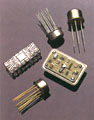 |
|
| SAC-TEC specializes in build-to-print and obsolete microcircuit technologies used in Aerospace applications. Having made a firm commitment to remain in the military and space components business, SAC-TEC continues to offer engineering options and long-term solutions to diminishing source parts problems. | |
Microcircuit Experience SAC-TEC has extensive experience in providing form, fit, and function devices either by using the original manufacturer's die as specified in SCD applications, or by emulating replacement circuitry using special wire bonding techniques and/or substitute technologies. SAC-TEC approaches every obsolete problem based upon available technology as follows:
Often newer technologies fail because they operate at faster speeds with switching times that are not recognized by older system designs. SAC-TEC finds it critical to become involved with the analysis of system timings and drive levels for these older components. In many cases, SAC-TEC's analysis of system applications has produced a recommendation for a replacement component. SAC-TEC has successfully provided replacement components for over 80% of customer requests when it appeared that none were available. Mask Set Misconceptions Contrary to the belief of many in the industry, the possession of an old mask set is not an answer to resurrecting old technology. These old mask sets do not mean old parts are manufacturable. Mask sets are designed for use on "one" specific silicon process line. Any change to that line, i.e. a new piece of equipment, a new wafer size or adding another process technology affects all the products run on that line. It is the old process with the old mask set and the old equipment that can produce obsolete devices. Likewise, many old processes have special "black box" features unique to each manufacturer. Applying an old mask set to a new or different wafer fab with different equipment and processing to newer techniques is identical to reinventing the integrated circuit from scratch. The design of a replacement microcircuit using today's CAD/CAM tools, newer semiconductor processing equipment lines and standardized wafer fabrication process rules can more practically produce a microcircuit on the first try. When using a 15-year-old mask set and process the re-inventing process may take up to four iterations to complete. Capabilities SAC-TEC operates a complete in-house manufacturing and testing facility and performs all assembly and screening to Mil-Std-883 or Mil-Std- 19500 process flows for both Class S and Class B quality levels. As long as some form of basic silicon die is obtainable, SAC-TEC is capable of manufacturing almost 80% of all semiconductors now offered in the industry for Hi-Rel applications. If the silicon is not available, SAC-TEC can substitute, emulate, or create "new silicon" designs that meet form, fit, or function replacements. All processes are developed to meet the same base line standards (i.e. burn-in, environmental, temperature/mechanical stress tests) as used by the major Hi-Rel companies like Harris, AMD, Motorola, and T.I. |
|
| Technology
Preservation Die/Wafer Bank: A Cost Effective Approach As defense contractors continue to downsize and more semiconductor manufacturers stop supporting the defense industry, the long-term continuation of many projects is now in jeopardy. Carrying a fully finished component inventory is often cost-prohibitive. Likewise, a forced redesign can be even more expensive. On the other hand, establishing a die/wafer bank could be a cost-effective approach to solving this technology availability problem. This approach minimizes program investment preserving your on-going technology while creating a pay-as-you-go program that meets your yearly product needs. SAC-TEC offers die/wafer banking of raw silicon microcircuits with custom builds of these circuits done on an as-needed basis. SAC-TEC provides long-term storage of silicon in bonded nitrogen containers. |
|
Technology |
||
| Custom Silicon Design | ||
| SRAM | ||
| EEPROM | ||
| Flash | ||
| DRAM | ||
| Microprocessors | ||
| Analog Circuits | ||
| Digital Circuits | ||
| Gate Arrays | ||
| Diodes | ||
| Transistors | ||
| Power Chips | ||
| MOSFET's | ||
| ASIC's | ||
| FPLA's | ||
| Resistor Arrays | ||
| Capacitor Arrays | ||
| Inductor Arrays | ||
Package Availability |
||
| Flat Packs | ||
| LCC's | ||
| Quad Packs | ||
| DIP's | ||
| Power Packs | ||
| PGA's | ||
| SIP's | ||
| J-Lead | ||
| Gull Wing | ||
| CERDIP's | ||
| RF Packages | ||
| Micro T's | ||
| Windowed | ||
Hi-Rel space and military applications |
||
| Better thermal characteristics | ||
| Smaller Footprints | ||
| Improved electrical characteristics | ||
| Maximum system capabilities | ||
Cost savings by utilizing successful older designs |
||
| Economical long-term problem solving | ||
| Minimize program cost --establish die/wafer bank | ||
| Capable of manufacturing almost 80% of all semiconductors for Hi-Rel application | ||